Seagate FireCuda Gaming 510 NVMe Review
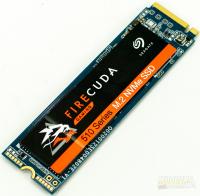 There’s no doubt that SSDs are faster than mechanical drives and faster still is the NVMe SSDs. We’ve known this for a while now. At CES, Seagate announced their FireCuda 510 series. This series contains a grand total of two products; a 1 TB NVMe drive and the 2 TB variant. Both FireCuda 510 drives are NVMe 1.3 compliant and take advantage of PCIe Gen 3 using 4 lanes. Unlike other vendors, the specifications between the two drives are very similar. Seagate states the sequential read speeds of the drives at 3450 MB/s and sequential write speeds of 3200 and 600,000 random write IOPS. Seagate is leveraging this drive towards gamers and content creators. It also boasts a massive 1300 TBW (Terabytes Written) coupled with a 5-year warranty, this drive should give even the most demanding user years of use.
As PCIe looms on the horizon, manufacturers will quickly be jumping on that technology as it allows them to push speeds even further. This drive is PCIe Gen 3 x4 and our sample came in the 1 TB flavor.
Specifications
| Standard Model (TCG Pyrite) | ZP1000GM30001 |
| Interface | PCIe G3 ×4, NVMe 1.3 |
| NAND Flash Memory | 3D TLC |
| Form Factor | M.2 2280-D2 |
| Sequential Read (Max, MB/s), 128KB | 3450 |
| Sequential Write (Max, MB/s), 128KB | 3200 |
| Random Read (Max, IOPS), 4KB QD32 T8 | 620,000 |
| Random Write (Max, IOPS), 4KB QD32 T8 | 600,000 |
| Terabytes Written (TB) | 1300 |
| Mean Time Between Failures (MTBF, hours) | 1,800,000 |
| Warranty, Limited (years) | 5 |
| Active Power, Average (W) | 5.3 |
| Idle Power PS3, Average (mW) | 20 |
| Low Power L1.2 mode (mW) | 2 |
| Temperature, Operating Internal (°C) | 0 to 70 |
| Temperature, Nonoperating (°C) | -40 to 85 |
| Shock, Nonoperating: 0.5ms (Gs) | 1500 |
| TRIM | Yes |
| S.M.A.R.T | Yes |
| Halogen Free | Yes |
| RoHS Compliance | Yes |
| Length, Max (mm) | 80.15 |
| Width, Max (mm) | 22.15 |
| Height, Max (mm) | 3.58 |
| Weight (g) | 8.1 |
My sample did not come in retail packaging. Seagate sent my drive in just a small antistatic bag. The FireCuda 510 is an M.2 2280 NVMe drive. This drive will fit into a standard M.2 NVMe slot on most motherboards and laptops. This drive is 1TB in capacity so both sides of the PCB are populated. On one side, Seagate has placed a sticker with the name of the drive series and their FireCuda logo.
On the other side of the drive, there is an additional sticker. It contains additional information such as serial and part numbers. The capacity of the drive is also listed here.
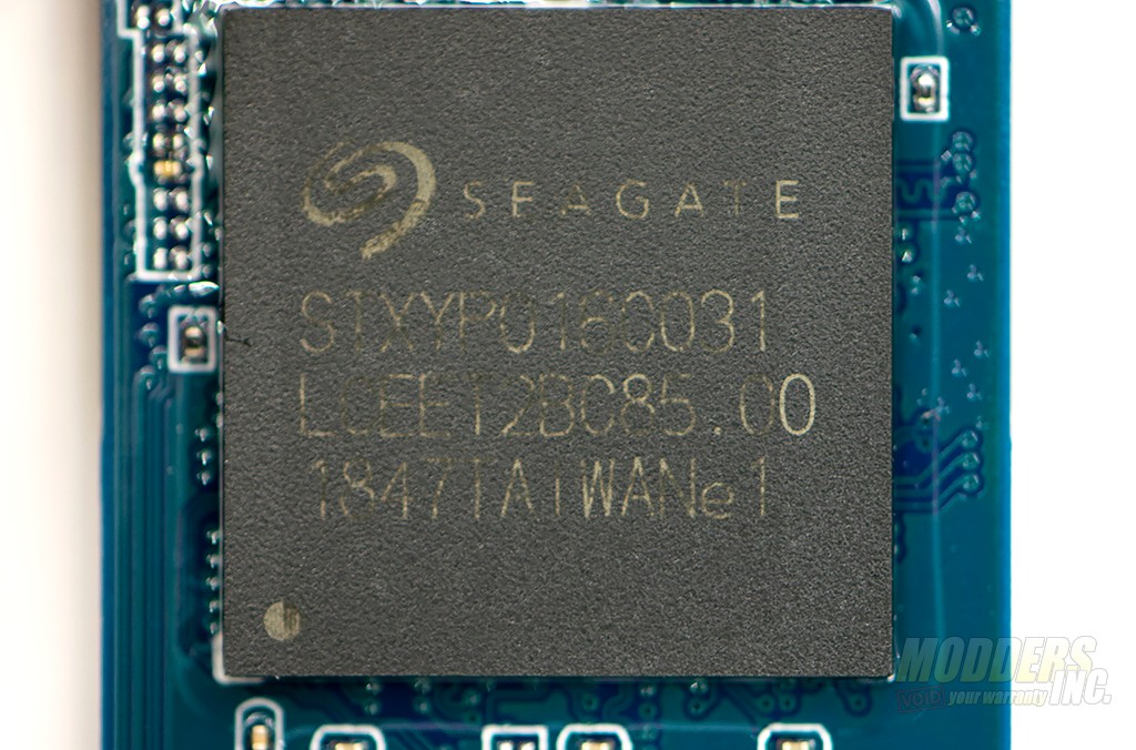
Peeling back the stickers reveals the ICs underneath. First up is the controller itself. While it’s labeled as a Seagate part, it is a rebranded Phison 5012-E12 controller. This controller is 8-channels and can support all the latest NAND. According to Phison, it supports SLC, MLC, TLC, and QLC as well as vertically stacked NAND.
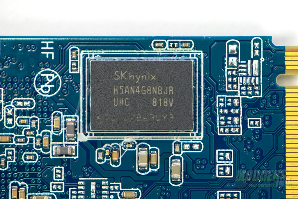
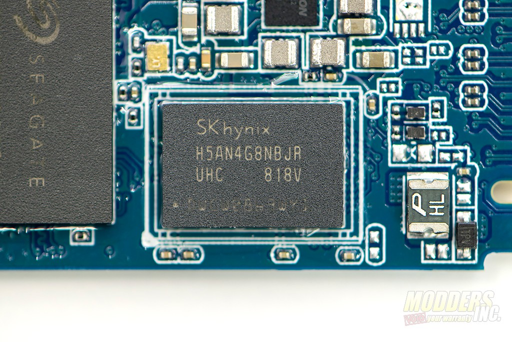
One each side of the PCB, there are two SKhynic H5AN4G8NBJA DRAM for a total DRAM buffer size of 1024.
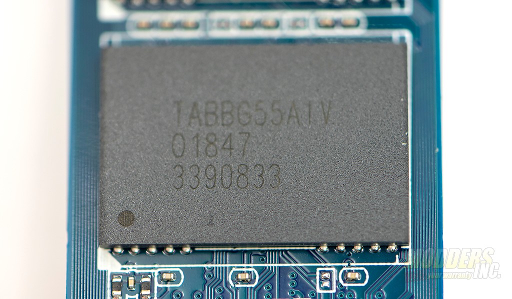
The PCB is populated with NAND flash ICs on both sides. The chips are labeled TABBG55A1V. These modules are manufactured by Toshiba and are in their 64-layer BICS 3D TLC product line. Each of the Toshiba modules is 256 GB in size. The endurance rating is 1300 TB.


